Surface Analysis and Microscopy

Discover our Capabilities
Electron Microscopy (SEM-EDX)
The scanning electron microscope (SEM) is a device for imaging surface structures. It provides images with high resolution and depth of field. Additionally, the distribution of various materials can be visualized. Furthermore, with the aid of Energy Dispersive X-ray Spectroscopy (EDX), the local elemental composition of the different sample areas can be analyzed.
Applications
- Structure and Composition of Components
- Failure Analysis
- Stains and Contaminants
- Analysis of Competitor Products
Surface Analysis (ESCA)
Electron Spectroscopy for Chemical Analysis (also XPS) analyzes (semi-quantitatively) the elemental composition of the uppermost nanometers (10-15 atomic layers) of solids.
The method also provides information about the bonding states of the elements. The removal of layers by sputtering allows for the measurement of the depth distribution of elements (depth profile).
Applications
- Adhesion
- Wetting Problems
- Coating Delamination
- Surface and Interface Characterization
- Corrosion Protection
- Reactivity of Catalysts
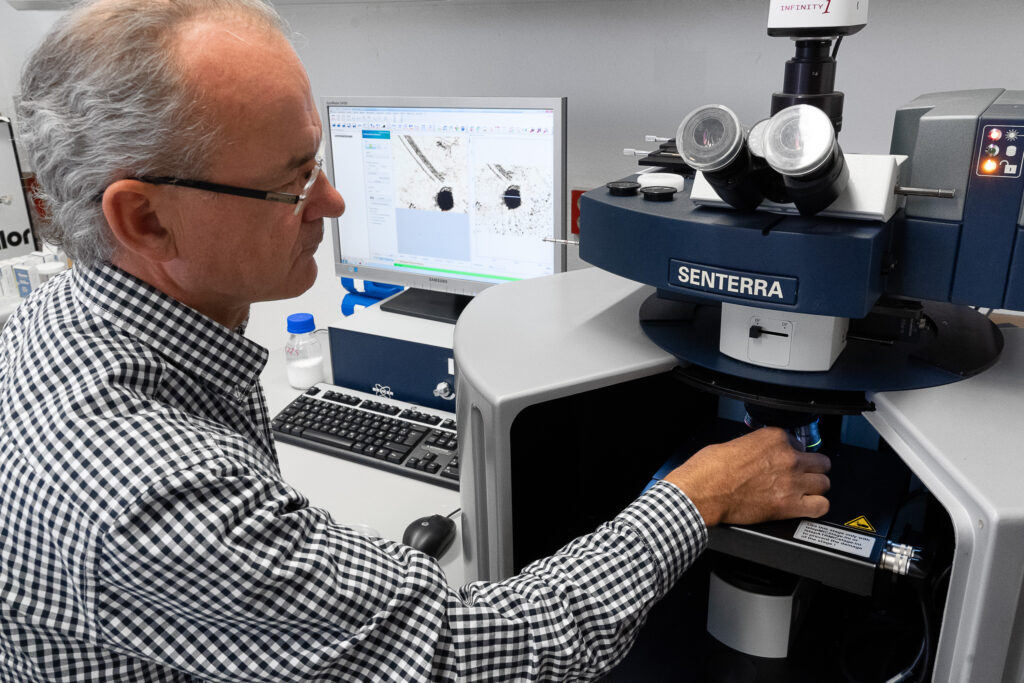
Molecular Spectroscopy (IR/Raman/UV-Vis)
In molecular spectroscopy, absorption or scattering of incident light occurs. This is characteristic of specific molecular fragments. The recorded spectra show specific bands for certain molecular components, allowing for the identification of organic materials in particular.
Applications
- Analysis of organic components
- Polymer Characterization
- Failure Analysis
- Stains and Contaminants
- Analysis of Competitor Products
Roughness Measurement (IR/Raman/UV-Vis)
Using a profilometer, the sample surface is scanned with a stylus of defined geometry, and standardized roughness parameters are calculated.
Applications
- Profile
- Waviness and Roughness
- Mean Roughness
- Bearing Ratio
- Roughness Depth
